
The first metasurface article published in Aftenposten, Norway’s largest printed newspaper
Original pdf article
Where are the Star Wars holograms?
Christopher Dirdal, Scientist, Microsystems and Nanotechnology, Sintef Digital
Knowledge is Aftenposten’s focus on research and science, where researchers and professionals from all over the country contribute articles.
The light of the sun keeps us warm, gives us food and clean energy, but also has a lot of credit for a number of the greatest achievements of science. For example, pioneering work in light research is the origin of today’s mobile telephone technology, Wi-Fi and the Internet of Things. And still, the development is happening at an amazing pace.
During an ongoing revolution in lighting technologies (photonics), I would like to ask some timely questions, such as:
1. Where are the Star Wars holograms?
Holograms are light projections of 3D images floating in the open air, such as that of Princess Leia in the iconic scene from Star Wars a New Hope from 1977 (!). Every time I see this scene I ask myself: Why do not such “living” holograms exist today?
The answer is basically simple and quite frustrating: So far, we have not found an adequate technology platform to control the light completely. In order to create a real living hologram, one must have complete control over two of the basic properties of light in real time: the light’s strength and phase (time shift). An enormous amount of research has been done to accomplish this, but existing technologies based on micro-mirrors and liquid crystals have difficulty becoming small enough to provide a wide field of view and good resolution.
However, there is a new hope: The Metasurfaces. These are textured surfaces, where the structures can be blocks or pillars of tiny dimensions, giving unmatched control over all the properties of light! The emergence of nanotechnology and powerful simulation tools over the last decade has given us a new field of expertise where development is happening very quickly.
One of the first metasurfaces used was precisely to create high-quality holograms that can have enormous potential in mobile phones and smart watches. Imagine if you could have FaceTime in the future with your loved ones floating in the air across the screen!
Metasurfaces can be used to create high quality holograms. It can have huge potential in cell phones and smart watches.
2. Why is optics big, heavy and expensive, while electronics are small, light and cheap?
There is something seriously wrong when I can fit a computer in my smart watch, but hardly fit the SLR camera in my luggage. How is it possible that optical systems are generally large, heavy and expensive, while electronics are so small, light and inexpensive?
The answer lies in how electronics are made: using mass production based on silicon technology. In the same way as the price per book fell like a stone after Gutenberg invented the 14th-century book press, the cost of transistors (basic components of the computer processor) has halved every two years since 1965. Today, billions of transistors can be made simultaneously on one disc made of silicon. In contrast, for example, large optical lenses are created by grinding thick glass discs, which must then be assembled with others with extreme precision. Here, the metasurface will lead to major changes: These can also be produced with silicon technology. At Sintef Microsystems and Nanotechnology, we use a technique called Nano-imprint lithography, which is basically similar to waffle frying: We stamp a pattern of rectangles in liquid plastic (polymer-resistant) and cure this. Then we etch away the bottom between the patterns. We are left with millions of rectangular pillars per square millimeter. The production of these metasurfaces is part of our research project ElastoMETA, funded by a bilateral research collaboration between Norway and Romania. The goal is to use metasurfaces for plastic detection. It is expected that by 2050, 12 billion tonnes of plastic waste will be buried in landfills or in nature.
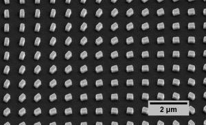

Image of a pre-processed metasurface (made by Sintef Microsystems and Nanotechnology in Oslotaken by electron microscope . The rectangular pillars have become about a thousand millimeters high after etching downwards between them. The area of the entire metasurface is 1.5 mm x 1.5 mm and contains more than 3,000,000 such pillars. The metasurface is intended to act as a lens for infrared light.
The idea behind our metasurfaces is to be able to create small and inexpensive sensors to recognize different types of plastic in distributed recycling stations. It will be crucial in a circular economy where reuse is an integral part of the economy.
3. What is the next major development in lighting technology?
Today, new and more advanced optical diagnostic techniques are being developed, such as studying brain activity or detecting cancer. The problem is that many of these need microscopes that are the size of coffee machines and are too large to place where they do most: namely inside the body! Also outside the body, optics should preferably be small. Today, there is great potential in being able to take pictures in 3D or to get information about the light spectrum (hyperspectral imaging). Applications include, for example, autonomous systems and precision farming. But again, many of these optical systems are far too large, expensive and energy-consuming to be placed on a small drone in the air or in the sea, for example. The opportunities metasurfaces provide for dramatically reducing optics could therefore lead to a revolution in medical diagnostics in the body and imaging of drones.